Hi,
since I’m thinking about upgrading my ground station with a 70cm antenna,
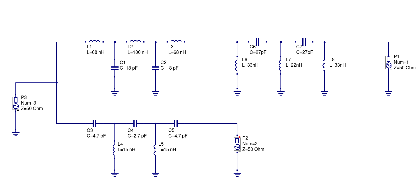
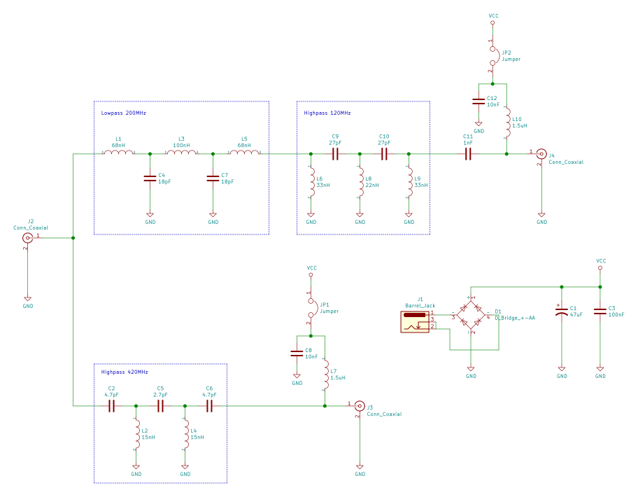
I decided try designing an antenna diplexer.
After some googling for existing schematics I came across the micro-diplexer by kw4fb, which has some really nice component values allowing it to be build from SMD components without winding your own inductors.
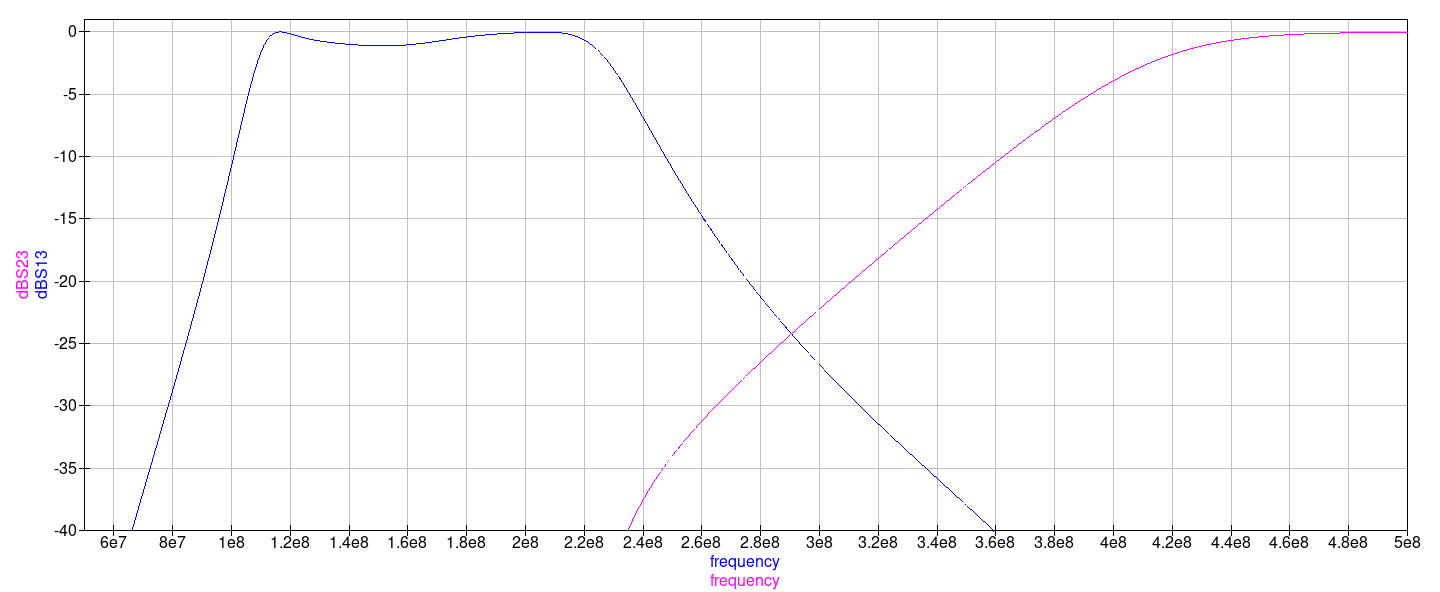
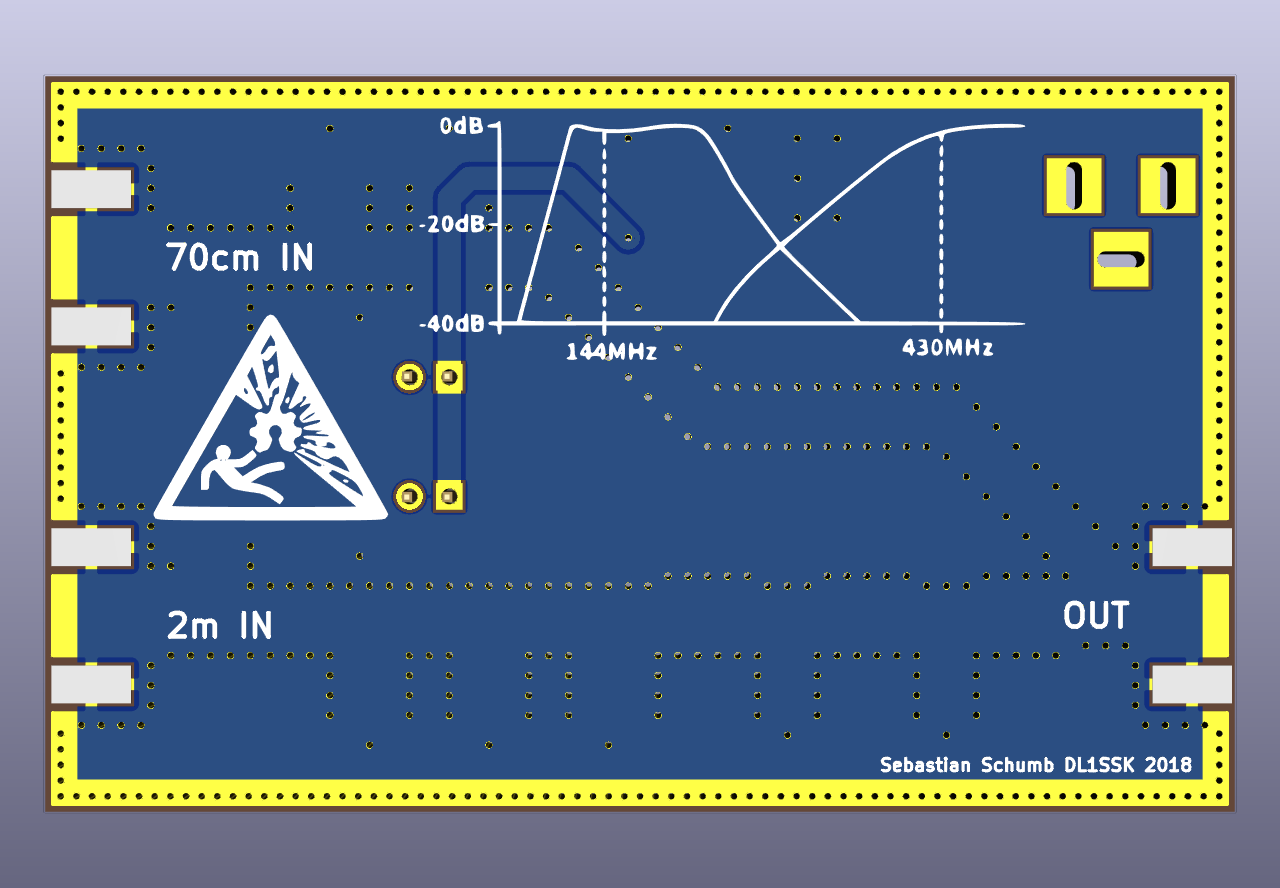
I took the design, added a lowpass filter to the 2m branch to get rid of some the strong FM broadcast stations in my area and plugged it into QUCS.
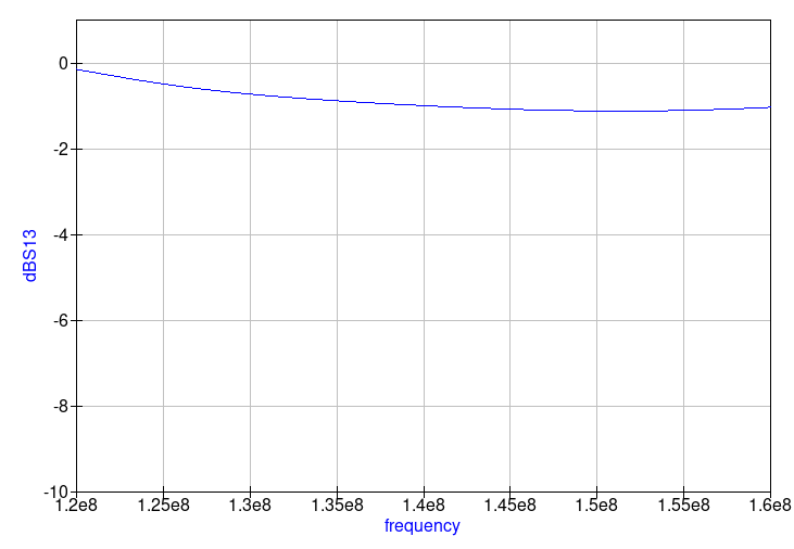
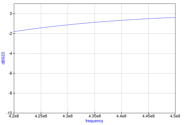
The passbands could be a little closer 0dB, but since I need two LNAs in front of it anyway I decided not to worry to much about it.
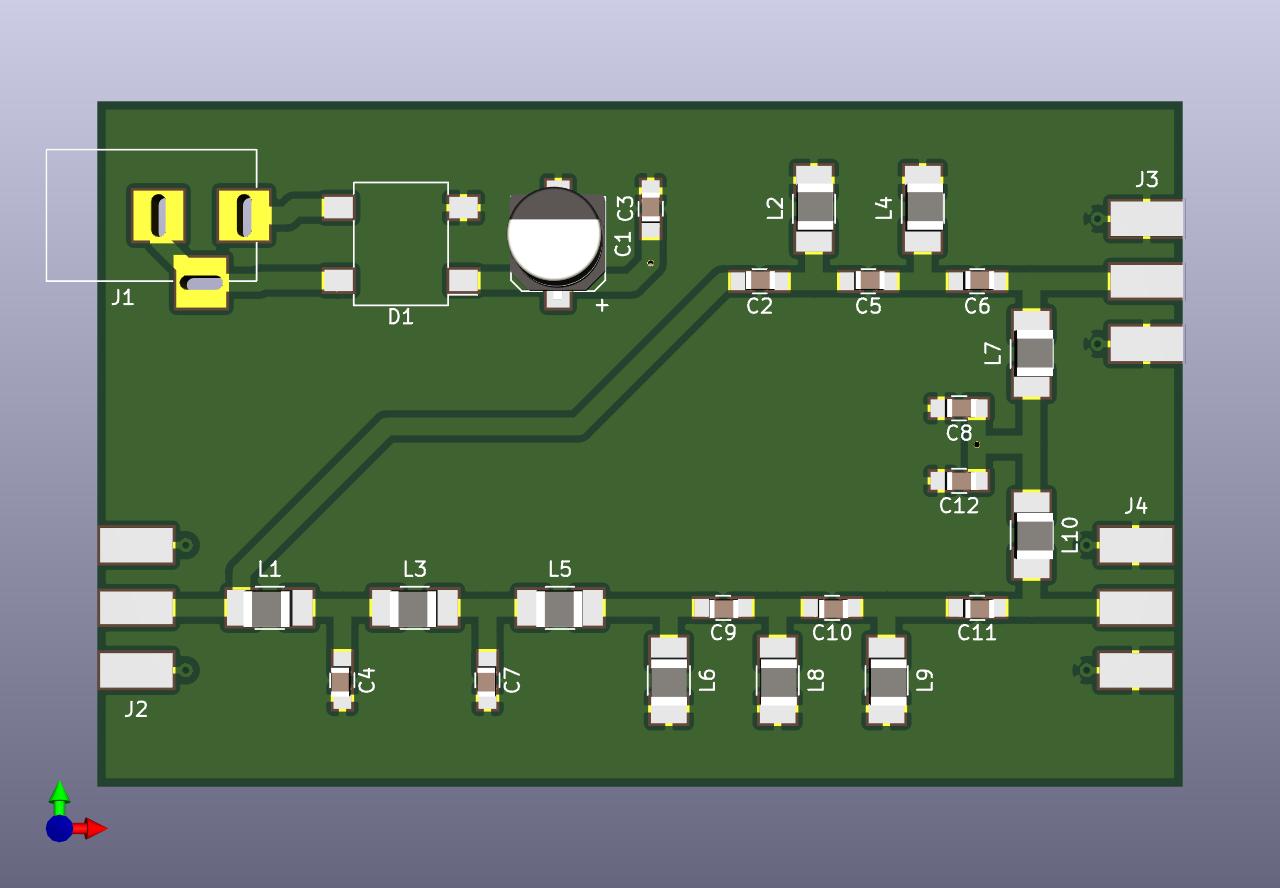
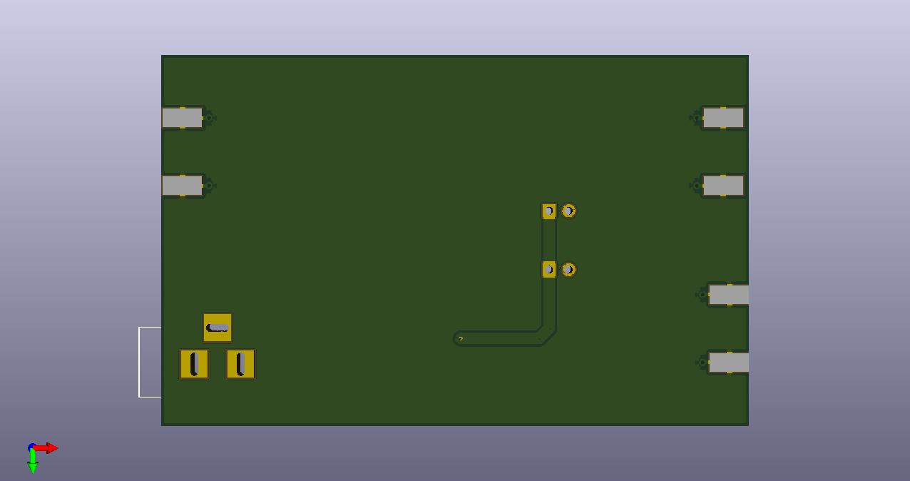
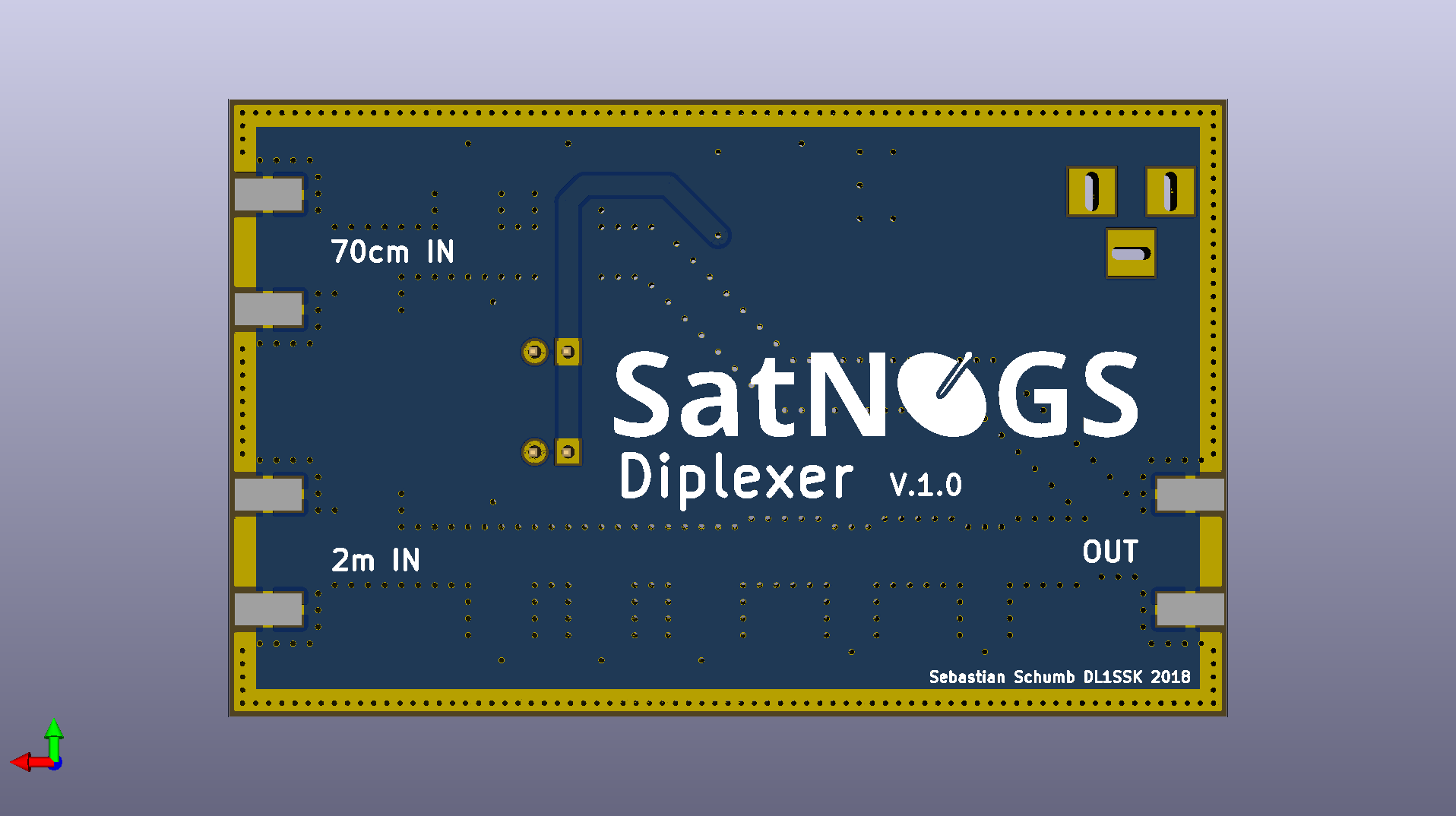
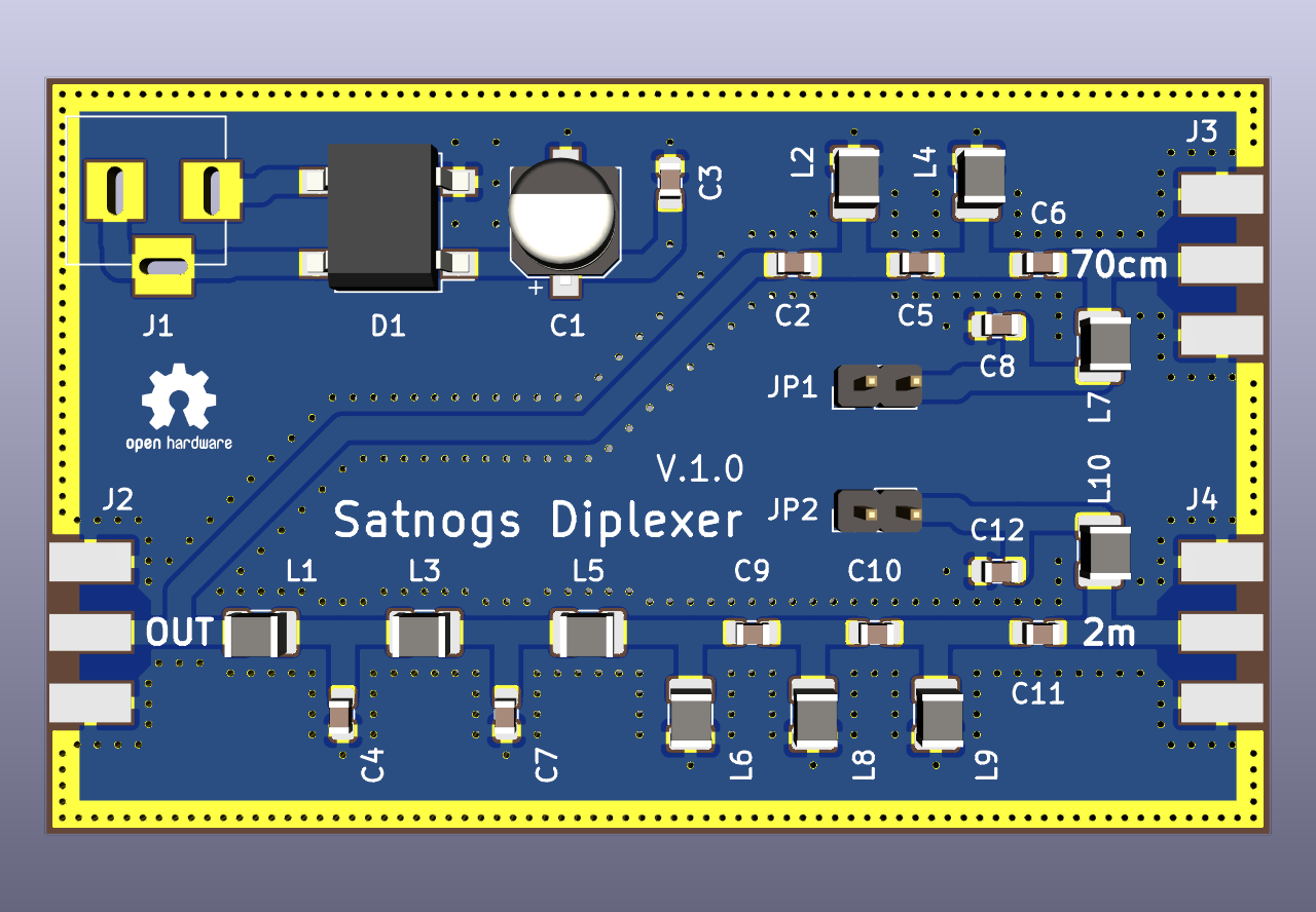
After @pjm’s suggestion in the IRC channel I decided to add two bias-tees for the antenna inputs and designed a first PCB in KiCad.
The layout is not yet final.
It certainly lacks a bunch vias connecting the ground planes.
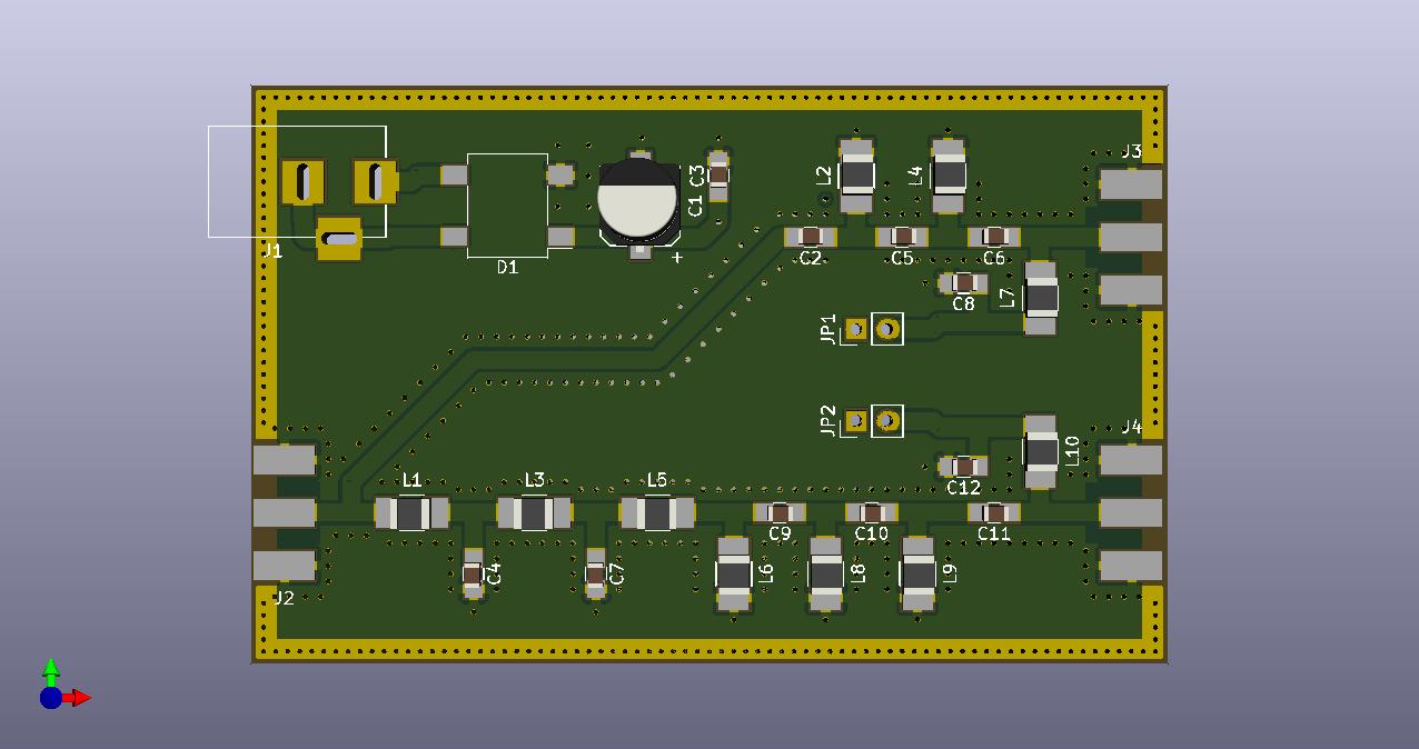
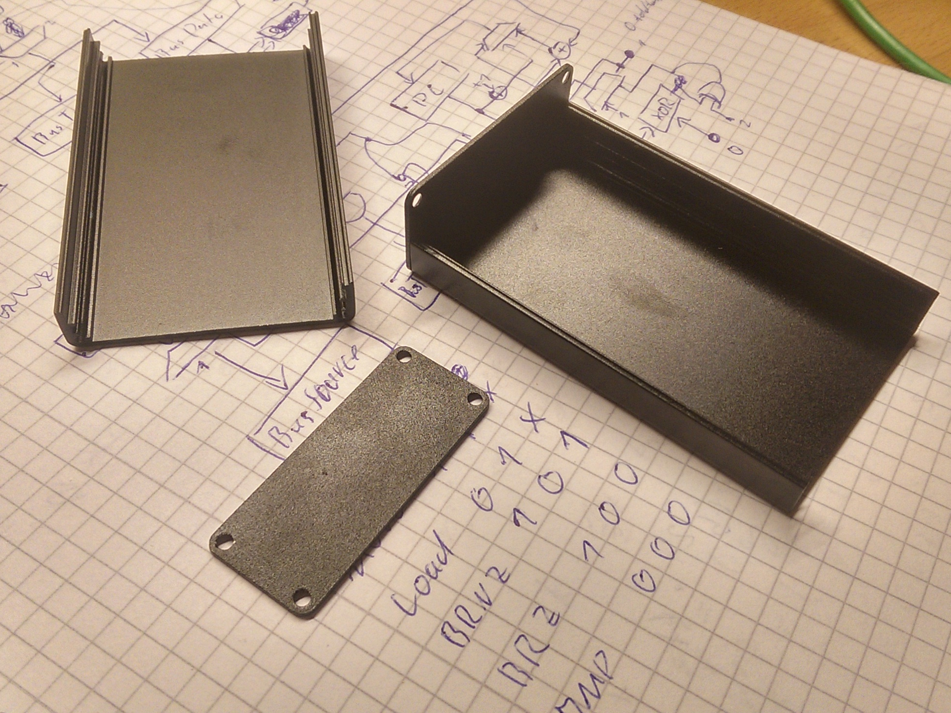
The dimensions of the board should fit a cheap aluminium housing I got from ebay some time ago.
(I know something ferromagnetic might be better, but on the other hand my SDR wrapped in plastic.)
I don’t have to much experience with designing PCBs for radio stuff,
some helpful comments and tips would be highly appreciated.
I think the trace connecting the output and the 70cm filters diagonally across the board looks a bit odd and might be to close to the power supply trace.
Also I’m not to sure about the way the two traces meet at L1.
This looks excellent. Double check the RF track widths using the calculator at http://www.emtalk.com/mscalc.php - You need to know some of the PCB parameters (Dielectric Constant (εr) and Dielectric thickness. For low frequencies the corner tapers on the microstrip wont matter at all, so what you have will be fine. It might be worth measuring the centre pin pad width and using the above calculator with that figure and the board εr to see if its 50ohm, and if so widen the other RF tracks. My only other comment would be that maybe its worth adding jumpers or links for power to each bias-tee output, i.e. I might use a QFH on the VHF port (which is a dead short) and a antenna on UHF that has an LNA.
You could also add a couple of fuses or polyfuses to prevent the bias-tee inductor going pop due to a mis-connect etc.
Since you are designing in KiCAD there is the PCB calculator tool in there with the RF Track calculator functionality (which works great!)
@ar3itrary I was wondering if it might worth it to have an integrated duplexer & LNA board, with the LNA sitting after the band-passes. I think pretty much everyone in the community would want to use it!
I’ve already using the calculator in KiCAD to get the initial parameters for the traces.
The one at http://www.emtalk.com/mscalc.php gives similar results.
Having the LNA on the same board is something I’ve been pondering for a while now.
The conventional wisdom seem to be that the LNA should ideally be placed as close to the antenna as possible and preferably before filters so it can make up for cable and insertion losses.
That would probably work fine for my ground station as it is located in small village,
surrounded by mountains on all sides which shield it it even from the local HAM radio relays.
On the other hand if you are in an urban area, or even worse an area with strong transmitters nearby, you’ll run into problems with this approach.
I’m currently in an urban area with strong American military transmitters nearby,
which operate close to the 2m band.
In that case the strong signals simply saturate you amplifier and the filter after it is basically useless.
So when I’m experimenting here it is better to have the filter in front of the LNA.
Having the diplexer/filter as separate module just provides some flexibility to pick what ever works best for given location.
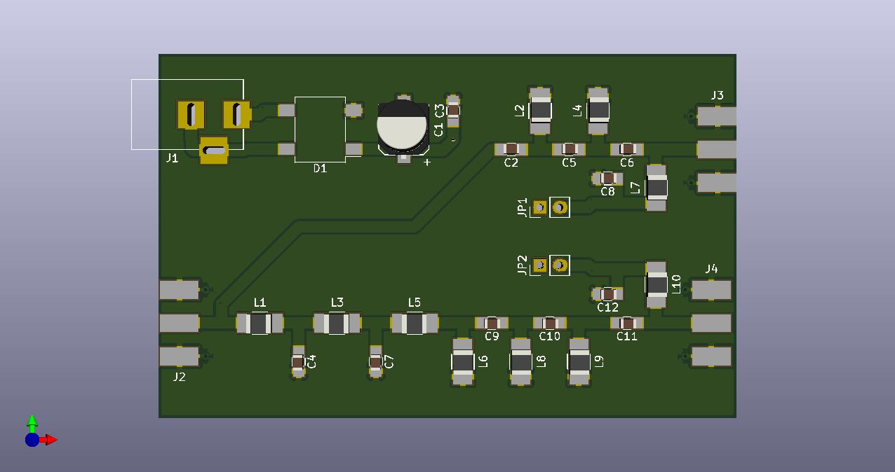
@pjm The jumper are probably a good idea.
My plan was to leave the inductor unpopulated, but being able to enable and disable the power without soldering sound better to me.
Given the large amount of free space on the board it should be trivial to add some jumpers.
So I found the parameters for the FR4 hidden somewhere on my PCB houses website. Er of 4.5, dielectric loss factor of 2e-2 and specific resistance of 1.72e-8.
Sounds an awful lot like they just copied the literature values, but I guess it will be close enough.
Using them I calculated a the parameters for a coplanar wave guide with goundplane.
Both calculators I tried gave me 1.5mm traces with 0.3mm space to the ground planes for
a 1.6mm board with 0.035mm copper on both sides.
I decided to prefer that to an actual microstrip line as it yields a little narrow traces (1.5mm instead of 2.1something mm) and it has the added benefit of being able to simply slap ground pour on both sides of the board.
It still lacks a few vias connecting the ground planes.
Yesterday I tried to read up on grounding and via placement for RF PCBs.
That’s an interesting rabbit hole … and a deep one.
I’ve encountered the full spectrum of opinions from “Unless you are dealing with >1GHz it’s probably going to work alright no matter what you do” to “Low impedance paths everywhere! Add All the vias or the RF voodoo gods will destroy the universe!”.
So I looked at some other board designs operating at similar frequencies,
which wasn’t really helpful either.
In the end I just added a lot of via everywhere.
To many surely won’t hurt, unless the board house complains.
Also it look like there is some serious high frequency stuff going on.
Thanks.
I’ve been using KiCAD since at least 2008 (at least that’s the earliest date I could find on one of my boards) so one might say I have ten years of experience now.
However I probably designed about 5 to 10 PCBs a year and KiCAD keeps getting new feature so there’s still a lot to learn.
Also since I’ve been asked about it elsewhere:
The cheap ebay enclosure can be found from various shops by searching for “aluminium 805020mm PCB enclosure”.
Its one of those clam shell things held together by its front and back plate.
@Zathras I used Qucs, the ‘quite universal circuit simulator’.
It has weird quirks in the time domain simulations, but the S-Parameter simulations are pretty good.
Same goes for the filter synthesis tool, which requires a little knowledge about filter design schemes.
I immediately recognized some terms from my theoretical university course on filter design,
so your user experience my vary.
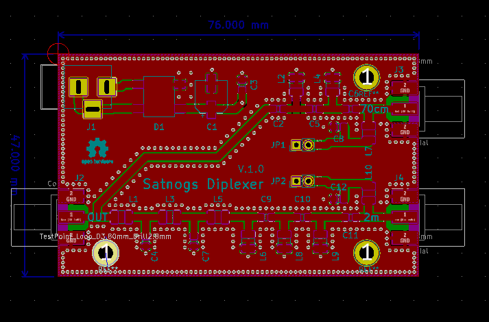
Some more updates on the enclosure & PCB dimensions:
I’m currently at my workshop with all my spare parts boxes, so that I can take some measurements on that enclosure.
Exact outer dimensions are: 82.5mm x 50.5mm x 20.5mm with both end plates on.
The space for the PCB is 80.2mm x 47.3mm x 1.8mm.
The SMA connectors that go on the PCB edge need 1.5mm extra space between the front plate and the PCB.
So the PCB dimensions should be around 77mm x 47mm to ensure a fit with some play.
My current draft is 78mm x 48mm so it will need some more fine tuning to get to final dimensions.
As the smallest number of boards at my current Chinese PCB manufacturer of least mistrust is 10 and I plan on doing a panel with 2 boards per panel, I’ll surely have a few spare PCBs, no problem.
Some goes for the components.
Those are all passives, so I’ll order them in larger quantities anyway (or I’ll have them laying around already since I ordered lots of spares last time.)
I’ll also order a stencil and reflow solder the boards so assembling a few more is not a big deal.
Ah ok, thanks.
Reason I ask that I might try to make the UHF section bandpass, for additional filtering.
I’ve never designed filters so an interesting experiment.
@Zathras The tricky bit is finding a combination of values that work well while also being of the E series so that you can buy the components.
I’ve build filters using air coils for the weird inductors I got using the design tool and well … let’s just say tuning it is a full afternoon of fun for the entire family.
So as a rule of thumb I prefer to sacrifice some selectivity for more practical component values.
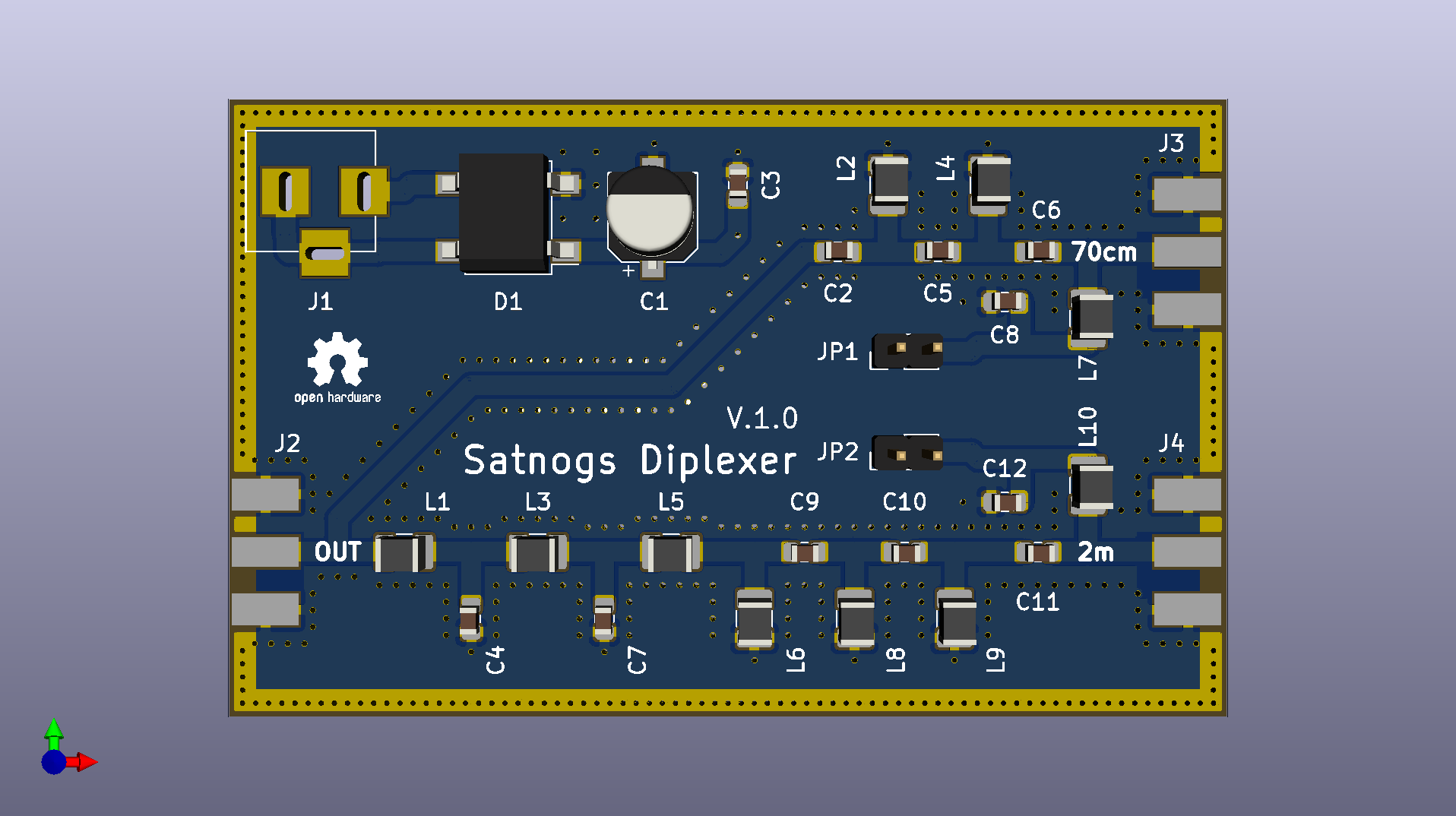
By the way: I made the board a few mm smaller, it’s now 76mm x 47mm so it should fit the enclosure perfectly.
Here is how a final version might look like.
The idea for logo on the back since is that I’ll have to pay for the silkscreen anyway, so I might as well do something cool.
On the other hand it makes the board look somehow official,which might cause some confusion, at least if I start handing out the spares to people.
I think should take that off again, before generating the gerbers.
Also I’m a fan of blue soldermask (green is boring, red to aggressive, white only gets dirty,
yellow usually has bad contrast to the silkscreen and you just can’t see the traces on black boards), so the boards will likely be blue.
I’ll check them again tomorrow (as I am very likely to miss a little detail after staring at the PCB for hours) and then send them of the board house, along with a few PCBs for another project.
Also I’ve added a proper licence and a readme to repo.
Luckily I didn’t get around to order the boards yet.
Mounting holes are probably a good idea … but adding holes in the corners will be hard.
There is enough space to squeeze 2mm hole in there with no space for a screw head.
In my experience 2mm mounting screws are utterly useless as you never have those small screws at hand.
Making space for M3 screws basically it means moving every connector
and therefore having to shift around everything on the board including most of the vias.
After that I’ll likely have to reiterate over all the minor tweaks I did this week.
That will keep me busy for a while.